Home > Tech Tools > Technical Papers > Selecting Film Bus Link Capacitors For High Performance Inverter Applications
Abstract – For years design engineers have chosen electrolytic capacitor technology for use as the bus link capacitor on inverter designs. The main attraction has always been the low cost per farad associated with electrolytic capacitors.
This paper will present a practical mathematical approach on how to properly size a bus link capacitor for a high performance hard switched DC to AC inverter using film capacitors and will show how film capacitors are advantageous over electrolytic capacitors in terms of size, weight, lifetime, inverter efficiency and cost.
I. INTRODUCTION
Electrolytic capacitors have been the workhorse technology for hard switched inverter bus link capacitors for many years. Electrolytic capacitor technology has also remained virtually unchanged over the years. Up till now, the greatest benefit in using electrolytic capacitors for bus link capacitors in inverters has been their cost. Electrolytic capacitors due however suffer from low ripple current capability due to high ESR and ESL, high thermal resistances limiting the ability to get the heat out, clumsy packaging sizes and mounting difficulties, weight, temperature range and limited lifetime.
Many high performance inverters such as electric vehicles, aircraft, and alternative energy to name a few are now turning to film capacitors because they do not have the limitations of electrolytic capacitors. Moreover, modern film capacitors not only perform better but can be a cost effective technology as well if applied correctly.
II. THE BUS LINK CAPACITOR’S ROLE
The bus link capacitor is used in DC to AC inverters to decouple the effects of the inductance from the DC voltage source to the power bridge. Figures 1A and 1B show two examples of a typical hard switched pulse width modulated (PWM) inverter that converts DC voltage to a three phase AC voltage. The bus link capacitor provides a low impedance path for the ripple currents associated with a hard switched inverter. The ripple currents are a result of the output inductance of the load, the bus voltage and the PWM frequency of the inverter. Unfortunately the ripple currents have been the primary factor in sizing the electrolytic bus link capacitor.
The bus link capacitor also plays a role in reducing the leakage inductance of the inverter power bridge. Leakage inductance in an inverter power bridge leads to inefficiencies due to the voltage spikes they produce when the power devices are switched on and off at a high rate of dI/dt. If the leakage inductance gets too large, the switching time of the power switches must be increased to keep the voltage spikes from damaging the power devices. Increasing the switching time of the power devices increases the turn on and turn off losses in each of the power switches contributing to more switching losses which manifest themselves in extra heat dissipation in the switching devices. Having a low impedance DC bus is fundamental for an efficient inverter design. The bus link capacitor’s internal ESL and external packaging is a key to reducing leakage inductance in the inverter power bridge.
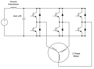 Fig. 1A: Three Phase Motor Drive
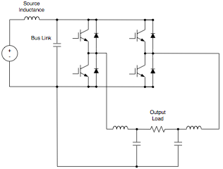 Fig. 1B: Single Phase DC to AC Voltage Inverter
III. BUS CAPACITANCE REQUIRED FOR INVERTERS
The first step in sizing capacitors for inverter bus link applications should be to understand how much bus link capacitance is required for a given inverter design. The biggest design limitation for electrolytic capacitors in inverter applications has been the amount of ripple current that the electrolytic capacitor can sustain. This limits the design criteria of the designer to figuring out how many individual capacitors are required for a given design rather than the total amount of capacitance that is required.
For example, let’s say for a given inverter, the bus link capacitor maximum ripple current requirement is 56 Arms. A 5,000uF / 450V electrolytic capacitor typically will only be able to sustain 28 Arms for a given package size. Therefore the designer must use two 5,000uF electrolytic capacitors totaling 10,000uF to meet the required 56 Arms capability. As will be seen further in this paper, 10,000uF is many times more capacitance then is required to meet the design performance for an inverter.
Having an excessive amount of bus link capacitance also presents some safety concerns. Once the inverter is powered down, a large amount of energy is stored in the bus link capacitor and this energy can be depending on the voltage, lethal if touched by an unsuspecting repair person. Most inverter designs with large amounts of capacitance add circuitry to discharge the bus link capacitors in a quick and safe manner upon power down so as not to present a safety concern. This of course adds complexity and cost to an inverter’s overall design.
Film capacitors do cost more per uF than electrolytic capacitors. It will be shown in this paper that the amount of capacitance needed for an inverter bus link capacitor design is much less for a film capacitor than an electrolytic capacitor since the film capacitor is not limited by ripple current rating like the electrolytic capacitor is. This is why when film capacitors are considered as direct uF replacements in an existing inverter design, the film capacitors will look much more expensive if you simply use the same amount of uF for film capacitors as you would with electrolytic capacitors.
IV. CALCULATING THE RIPPLE CURRENT
Referring to Figure 2, the source inductance is usually large enough to limit the high frequency ripple current. Therefore the ripple current in the bus link capacitor is essentially the same as the ripple current in the phase leg as illustrated in Figure 2. When the top left and bottom right switches are turned on the current flows from the bus link capacitor through the load via top left and bottom right switches and returns to the bus link capacitor. Similarly, the current flows from the bus link capacitor through the load when the bottom left and top right switches are turned on.
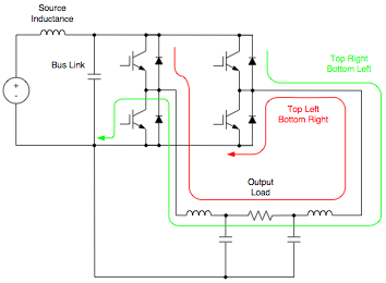 Fig. 2: PWM Ripple Current Flow
The output voltage of a single totem pole or leg is a series of PWM signals with the amplitude of either the bus voltage or bus common as shown in Figure 3. The output voltage Vout is shown for a voltage inverter and a motor drive inverter.
The output voltage Vout, is defined by the following equation;
Vout = duty cycle ∗ Vbus (1)
Where the duty cycle is a value from 0 to 1 and is in reference to the top switches on time.
For convenience let;
duty cycle = d (2)
Therefore;
V=d∗V (3)
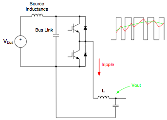 Fig. 3A: Single Phase Voltage Inverter Leg
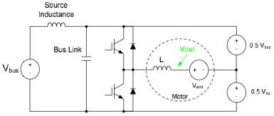 Fig. 3B: Single Motor Drive Inverter Phase Leg
When the top switch is turned on, the voltage is applied across the load inductor L is defined as VL . The current in the inductor L will integrate up at a rate that is determined by the voltage and inductance as defined in the following equation;
VL = L ∗ (dI/dt) (4)
Rearranging equation (4) yields;
dI = VL/L ∗ dt (5)
Integrating with respect to t;
∫ dI = ∫ VL/L ∗ dt (6)
ΔI=VL/L∫ dt (7)
ΔI = (VL) ∗ (Δt) /L (8)
Where L is the inductance in Henries and Δt is the top switch on time in seconds.
When the top switch is turned on;
VL = Vbus – Vout (9)
Substituting in equation (9) into (8) yields;
ΔI=(Vbus -Vout )∗(Δt)/L (10)
Substituting in equation (3) into (10) yields;
ΔI=(Vbus –(d∗Vbus ))∗(Δt)/L (11)
The top switch on time can be defined as;
Δ t = d ∗ PWM period (12)
or
Δ t = d ∗ 1/PWM Frequency (13)
Let’s define the PWM frequency as f. so therefore;
Δ t = d ∗ 1/f (14)
Substituting in equation (14) into (11) yields;
ΔI=(Vbus –(d∗Vbus))∗(d)/(f∗L) (15)
Simplifying equation (15) yields;
ΔI = d ∗ (1– d) ∗ Vbus / (f ∗ L) (16)
Figure 4 is a plot of Vbus/(f∗L)orΔI,versesd. This plot shows that the maximum Vbus / (f ∗ L) verses d occurs when d is equal to 0.5 or 50% duty cycle.
Therefore, the maximum ΔI is when the duty cycle (d) is 50%.
Substituting in 0.5 for d in equation (16) yields;
ΔI 0.5t = 0.5 ∗ (1– 0.5) ∗ Vbus / (f ∗ L) (17)
ΔI 0.5t = 0.25 ∗ Vbus / (f ∗ L) (18)
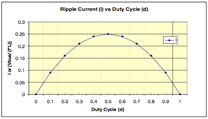 Fig. 4: ΔI vs Duty Cycle (d)
V. CALCULATING THE BUS LINK CAPACITOR RIPPLE VOLTAGE
Now that the ripple current in the bus link capacitor is known, it is now simple to calculate the resulting bus link capacitor ripple voltage.
A capacitor’s current (iC) is expressed as;
iC = C ∗ (dV/dt) (19)
Where C is the capacitance in Farads, and dV/ dt is the rate of change in voltage with respect to time. Rearranging the equation and solving for dV yields;
dV=(iC /C)∗dt (20)
Since iC = ΔI 0.5t
iC =ΔI0.5t = 0.25∗Vbus/(f∗L) (21)
Substituting in equation (18) into equation (20) yields;
dV = [0.25 ∗ Vbus / (f ∗ L ∗ C)] ∗ dt (22)
∫dV= ∫[0.25∗Vbus/(f∗L∗C)]∗dt (23)
ΔV0.5t = [0.25∗Vbus/(L∗C)]∗ ∫(1/f)dt (24)
Since 1/f = t;
ΔV0.5t = [0.25∗Vbus/(L∗C)]∗∫(t)dt (25)
ΔV0.5t = [0.25∗Vbus/(L∗C)]∗ (Δt2 /2) (26)
ΔV0.5t = [(Vbus /(8∗L∗C)] ∗ (Δt2 ) (27)
Using the Δt for a 50% duty cycle;
Δt = 0.5 t = 1 / (2 ∗ f ) (28)
ΔV0.5t = Vbus /(32∗L∗C∗f2 ) (29)
Where ΔV0.5t is the maximum peak to peak ripple voltage across the bus link capacitor at a 50% PWM duty cycle, Vbus is the bus voltage, L is the phase inductance in Henries, C is the bus link capacitance in Farads, and f is the PWM frequency in Hertz.
VI. GENERAL DESIGN EXAMPLE
So let’s make the assumption that the ripple current capability of the bus link capacitor will not be a limiting factor like it is with electrolytic capacitors. We see from what was previously discussed that the ripple current is only defined by the bus voltage, the load inductance, the duty cycle and the PWM switching frequency (see equation (16) above). From equation (18) we can determine the maximum ripple current which occurs at a 50% duty cycle. We then calculate the maximum bus link capacitor ripple voltage which is at a 50% duty cycle (see equation (29). This is a critical point since once the ripple current does not become a limiting factor, the bus link capacitance selection is based on the maximum bus ripple voltage desired.
Using equation (29), Figure 5 shows a plot of bus ripple voltage verses bus link capacitance for a bus voltage of 325 volts, a phase load inductance of 100uH and a PWM switching frequency of 10 kHz. Note that there is a diminishing return on bus ripple voltage verses capacitance after a certain amount of bus link capacitance. So beyond a certain point, adding capacitance does little to enhance the performance of the inverter.
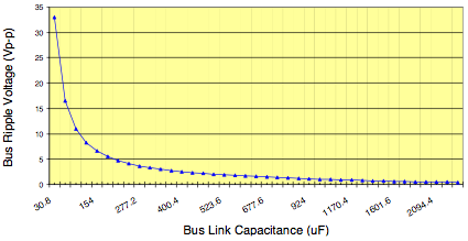 Fig. 5: General Design Example Bus Ripple Voltage vs Bus Link Capacitance
In this same example, if an electrolytic capacitor was used, the capacitance would be based solely on ripple current. Using the above parameters for bus voltage, load inductance and PWM switching frequency, and using equation (18) to calculate bus capacitor ripple current, the bus ripple current yields;
ΔI 0.5t = 0.25 ∗ Vbus / (f ∗ L) (18)
Substituting the values in yields;
ΔI 0.5t = 0.25 ∗ 325 / [(10 ∗ 103 ) ∗ (100 ∗ 10-6)]
ΔI 0.5t = 81.25 Ap-p or 28.7 Arms
If an electrolytic capacitor were sized for this application it would require a 5,000uF / 450V capacitor to meet the ripple current requirement at 10 kHz switching frequency. Using equation (29), the amount of ripple voltage on the bus in this case would be;
ΔV0.5t = Vbus /(32∗L∗C∗f2 ) (29)
ΔV0.5t =325/[32∗(100∗10-6)∗(5∗10-3)∗(10∗103)2 ]
ΔV0.5t = 0.20 Vp-p!
That’s less than 0.1% voltage ripple on the bus! So what is a reasonable amount of ripple voltage on the bus? Certainly 1% would be acceptable. Referring to the chart in Figure 5 and rearranging equation (29) in terms of the capacitance needed for 3.3 Vp-p would be;
C= Vbus /(32∗L∗ΔV0.5t ∗f2 )
C= 325/[32∗(100∗10-6)∗(3.3)∗(10∗103)2 ]
C= 308 uF
That’s 16 times less capacitance than that of the electrolytic capacitor! Certainly packaging a 308 uF capacitor verses a 5,000uF capacitor makes for a smaller, lighter and more compact design.
If the actual allowable voltage ripple was 3%, the actual capacitance required is only 104μF! This application could actually be done with a 150μF, 500vdc UL34Q157K. This capacitor is only 40mm height with higher current, efficiency and life ratings; lower ESR, ESL, weight, volume and cost.
TABLE 1.
ELECTROLYTIC VS DRY FILM POLYPROPYLENE
PARAMETER COMPARISION
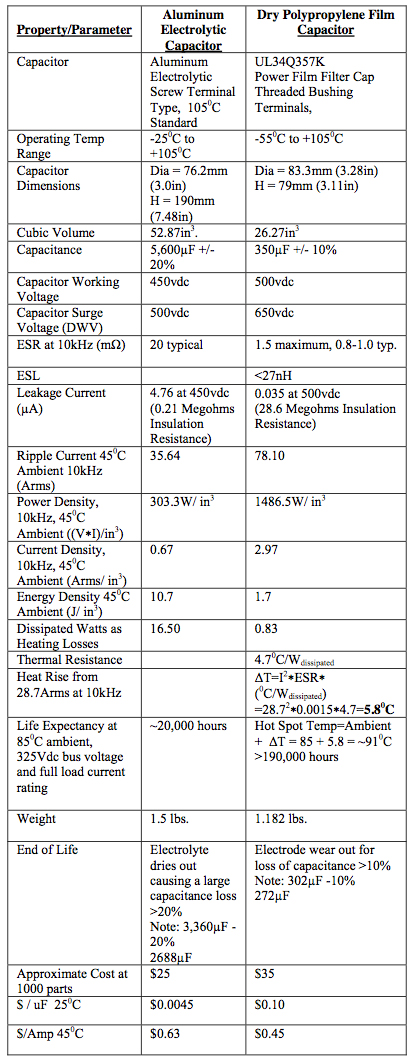
VII. 600KVA WINDMILL INVERTER DESIGN EXAMPLE
In the following representative example a customer wants to replace a bank of aluminum electrolytic capacitors with dry polypropylene film capacitors for an inverter bus link capacitor used in a 600KVA windmill application. The inverter has an output inductance of 380μH per phase and a nominal DC bus voltage of 680 volts. The switching frequency is 3kHz and the ripple voltage must be controlled to within 1% of the bus voltage. The ambient temperature requirements are 45oC – 60oC typical for 80% of application life and 850C for 20% of application life.
The present solution uses twelve aluminum electrolytic capacitors arranged in a series-parallel array to meet the voltage and current requirements.
Each discrete aluminum electrolytic capacitor has these ratings:
- Capacitance: 3,300μF
- DC Voltage: 350V
- Peak Voltage: 400V
- Max. Ripple Current at 3kHz: 19.44Arms
- ESR: 20mΩ
- Temperature rating: -250C to +1050C
- Diameter: 63.5mm (2.500”)
- Length:110mm (4.331”)
The 3-series by 4-parallel aluminum electrolytic capacitor bank ratings:
- Each leg contains 3 capacitors in series providing a working voltage rating of: 350Vdc ∗ 3 = 1,050Vdc
- Peak Voltage: 400Vdc ∗ 3 =1,200Vdc
- There are 4 parallel legs providing a ripple current capability of: 19.44 Arms ∗ 4 = 77.8 Arms
- Bank Capacitance of 3-series by 4-parallel legs: (3,300uF / 3) ∗ 4 = 4,400μF
- Bank ESR:(20mΩ∗3)/4=15mΩ
- Bank Length ∗ Width ∗ Height (includes 20mm clearance around case diameter for mounting bracket): 294mm ∗ 221mm ∗ 110mm = 7.15 liters (436.14in3)
To analyze this design let’s determine the ripple current requirement for this application. From equation (18) we can determine the maximum ripple current which occurs at a 50% duty cycle.
ΔI 0.5t = 0.25 ∗ Vbus / (f ∗ L) (18)
Substituting the values in yields;
ΔI 0.5t = 0.25 ∗ 680 / [(3 ∗ 103 ) ∗ (380 ∗ 10-6)]
ΔI 0.5t = 149.1 Ap-p or 52.7 Arms
The electrolytic capacitor bank has a capability of 77.8Arms so this capacitor bank is only operating at:
(52.7 Arms / 77.8 Arms) ∗100 = 68% of it’s rating for ripple current.
We then calculate the maximum bus link capacitor ripple voltage which is at a 50% duty cycle. From equation (29):
ΔV0.5t = Vbus /(32∗L∗C∗f2 ) (29)
ΔV = (680)/ [32∗(380∗10-6) ∗ (4.4∗10-3) ∗ (3∗103 )2 ]
ΔV0.5t = 1.41 Vp-p
That’s about 0.2% voltage ripple on the bus. The application calls for a 1% regulation on the bus or 6.8Vp-p. Rearranging equation (29) in terms of the capacitance needed for 6.8 Vp-p would be;
C= Vbus /(32∗L∗ΔV0.5t ∗f2 )
C= 680/[32∗(380∗10-6)∗(6.8)∗(3∗103)2 ]
C= 914uF
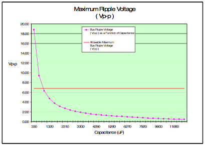 Fig. 6: Ripple Voltage verses Bus Link Capacitance for the 600 kVA Windmill Application.
The following are two examples of a film capacitor solution for the windmill inverter bus link capacitor application.
First the standard part solution is a standard package UL34 Series Power Polypropylene Film product which have the following specifications:
- Capacitance: 500μF
- DC Voltage: 1,100
- Peak Voltage: 1,320
- Ripple Current at 3kHz: 126Arms at 450C, 74Arms at 850C
- ESR: 1.5mΩ maximum, 0.8-1.0 typical
- ESL: 45nH typical
- Resonant Frequency: 33.55kHz
- Thermal Resistance: 3.480C/Wdissipated
- Diameter: 120mm (4.724”)
- Length:100mm (3.937”)
2-parallel film capacitor bank ratings:
- Bank Capacitance of 2-parallel legs: 1,000μF
- Bank Discrete Capacitors Required: 2
- Bank DC Voltage: 1,100
- Bank Peak Voltage: 1,320
- Bank Ripple Current Capability at 3kHz: 252Arms at 450C, 148Arms at 850C
- Bank ESR: 0.75mΩ maximum, 0.4-0.5 typical
- Bank ESL: 23nH typical
- Bank Resonant Frequency: 33.55kHz
- Bank Length ∗ Width ∗ Height (includes 10mm air spacing between parts): 260mm ∗ 130mm ∗ 100mm = 3.38 liters (206.26in3)
- Bank Dissipated Watts: 52.712 ∗ 0.0005 = 1.39Wdissipated • Bank Temperature Rise from Dissipated Wattage: 1.39Wdissipated ∗ 3.480C/Wdissipated = 4.80C
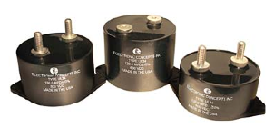 Fig. 7: Standard Product UL34 Series Power Polypropylene Film
The second film bus link capacitor solution is a UL9 series custom design single package unit with reduced ESR and ESL. A typical package form factor is shown in Figure 8.
Custom UL9 Series film capacitor ratings:
- Capacitance: 1,000μF
- DC Voltage: 1,100
- Peak Voltage: 1,320
- Ripple Current Capability at 3kHz: 252Arms at 450C, 148Arms at 850C
- ESR: 0.75mΩ maximum, 0.4-0.5 typical
- ESL: <20nH typical
- Bank Resonant Frequency: 50.33kHz
- Length ∗ Width ∗ Height: 203mm ∗ 165mm ∗ 89mm = 2.98 liters (182 in3)
- Dissipated Watts: 52.712 ∗ 0.0005 = 1.39Wdiss
- Temperature Rise from Dissipated Wattage: 1.39Wdissipated ∗ 2.520C/Wdissipated = 4.80C
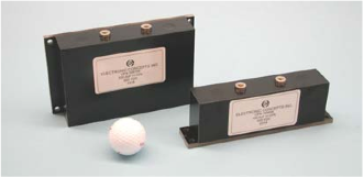 Fig. 8: UL9 Series Custom Design Polypropylene Film Unit with Reduced ESR and ESL.
TABLE 2.
WINDMILL INVERTER BUS LINK CAPACITOR BANK PARAMETER COMPARISION

The cost, volume, weight and efficiency of either of the film solutions presented offer a clear advantage over the aluminum electrolytic capacitor bank. The life expectancy of the film capacitors is at least 5x the aluminum electrolytic capacitors. Considering the labor savings of reduced assembly time and number of connections combined with the minimal bus work required versus the aluminum electrolytic capacitor bank and the savings at a system level is substantial. Field service costs become a fraction of those with the aluminum electrolytic capacitors offering an increased after market value. Additionally the film solutions can have value added functions such as the patented technologies of “Fuseac®” and “Control-cap”. Fuseac® technology employs a series disconnect thermal fuse which will open when the capacitor exceeds 1050C in the hot spot. Control-cap technology uses embedded sensors to provide control signals back for diagnostic alerts or controlled power- down or other system level actions.
VIII. SYSTEM CONSIDERATIONS
So far, this paper has limited the discussion of sizing of a bus link capacitor by defining the worst case ripple current in terms of the load inductance, bus voltage and switching frequency for a hard switched DC to AC inverter. However there are other factors that can affect and ultimately determine the bus link capacitance value. Some immediate examples are bus ripple voltage due to the AC to DC input rectifier circuit, regenerative energy, source impedance and load dynamics.
This paper will not and cannot address all the system affects on the bus link capacitor since they are unique to the application and depend on each specific design. This paper can provide however the opportunity to size the bus link capacitor by taking into consideration the effects of the bus voltage, load inductance and switching frequency. The designer can then analyze separately the effects of the other system dynamics to the bus link capacitor which can be added together with the worst case ripple calculation discussed in this paper and then determine the total bus link capacitance required for the unique design requirements.
IX. CONCLUSION
This paper has presented a discussion on how to properly size a bus link capacitor for a high performance hard switched DC to AC inverter using film capacitors and has shown that film capacitors are advantageous over electrolytic capacitors in terms of size, weight, lifetime, inverter efficiency and cost.
The supporting equations to determine the capacitance and ripple current requirements for an inverter were shown to be based primarily on bus voltage, load inductance and inverter switching frequency. The film capacitor technology has been shown to be smaller, lighter, have longer life and be cost competitive compared to the electrolytic capacitor technology for high performance inverter applications. Design examples were presented showing the advantages of film capacitors for a general inverter design and also a windmill inverter application.
Although this paper does not attempt to address every system consideration when designing a high performance inverter, it has discussed how to effectively size film capacitors in terms of ripple current, bus ripple voltage and load inductance as capacitor performance factors in selecting bus link capacitors. The result as compared to an equivalent design using electrolytic capacitors shows film capacitors used for bus link capacitors in hard switched inverters as being superior in terms of size, weight, lifetime and cost.


